(China (Mainland))

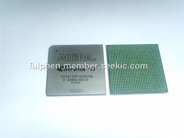
Product Summary
The EP2S130F1020C5N is an FPGA based on a 1.2-V, 90-nm, all-layer copper SRAM process and features a new logic structure that maximizes performance, and enables device densities approaching 180,000 equivalent logic elements (LEs). The EP2S130F1020C5N offers up to 9 Mbits of on-chip, TriMatrix memory for demanding, memory intensive applications and has up to 96 DSP blocks with up to 384 multipliers for efficient implementation of high performance filters and other DSP functions. Various high-speed external memory interfaces are supported, including double data rate (DDR) SDRAM and DDR2 SDRAM, RLDRAM II, quad data rate (QDR) II SRAM, and single data rate (SDR) SDRAM.
Parametrics
EP2S130F1020C5N absolute maximum ratings: (1)VCCINT, Supply voltage With respect to ground: 0.5 to 1.8 V; (2)VCCIO, Supply voltage With respect to ground: –0.5 to 4.6 V; (3)VCCPD, Supply voltage With respect to ground: –0.5 to 4.6 V; (4)VCCA, Analog power supply for PLLs With respect to ground: –0.5 to 1.8 V; (5)VCCD, Digital power supply for PLLs With respect to ground: –0.5 to 1.8 V; (6)VI, DC input voltage: –0.5 to 4.6 V; (7)IOUT, DC output current, per pin: –25 to 40 mA; (8)TSTG, Storage temperature No bias: –65 to 150℃; (9)TJ, Junction temperature BGA packages under bias: –55 to 125℃.
Features
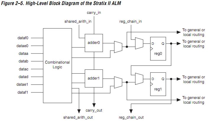
EP2S130F1020C5N features: (1)15,600 to 179,400 equivalent LEs; (2)New and innovative adaptive logic module (ALM), the basic building block of the Stratix II architecture, maximizes performance and resource usage efficiency; (3)Up to 9,383,040 RAM bits (1,172,880 bytes) available without reducing logic resources; (4)TriMatrix memory consisting of three RAM block sizes to implement true dual-port memory and first-in first-out (FIFO) buffers; (5)High-speed DSP blocks provide dedicated implementation of multipliers (at up to 450 MHz), multiply-accumulate functions, and finite impulse response (FIR) filters; (6)Up to 16 global clocks with 24 clocking resources per device region; (7)Clock control blocks support dynamic clock network enable/disable, which allows clock networks to power down to reduce power consumption in user mode; (8)Up to 12 PLLs (four enhanced PLLs and eight fast PLLs) per device provide spread spectrum, programmable bandwidth, clock switch-over, real-time PLL reconfiguration, and advanced multiplication and phase shifting; (9)Support for numerous single-ended and differential I/O standards; (10)High-speed differential I/O support with DPA circuitry for 1-Gbps performance; (11)Support for high-speed networking and communications bus standards including Parallel RapidIO, SPI-4 Phase 2 (POS-PHY ; (12)Level 4), HyperTransport? technology, and SFI-4; (13)Support for high-speed external memory, including DDR and DDR2 SDRAM, RLDRAM II, QDR II SRAM, and SDR SDRAM; (14)Support for multiple intellectual property megafunctions from Altera MegaCore functions and Altera Megafunction Partners Program (AMPPSM) megafunctions; (15)Support for design security using configuration bitstream encryption Support for remote configuration updates.
Diagrams
| Image | Part No | Mfg | Description |  |
Pricing (USD) |
Quantity | ||||||
|---|---|---|---|---|---|---|---|---|---|---|---|---|
 |
 EP2S130F1020C5N |
|
IC STRATIX II FPGA 130K 1020FBGA |
Data Sheet |
|
|
||||||
| Image | Part No | Mfg | Description | |
Pricing (USD) |
Quantity | ||||||
 |
EP2S |
Other |
|
Data Sheet |
Negotiable |
|
||||||
|
EP2S130F1020C3 |
|
IC STRATIX II FPGA 130K 1020FBGA |
Data Sheet |
|
|
||||||
|
EP2S130F1020C3N |
|
IC STRATIX II FPGA 130K 1020FBGA |
Data Sheet |
|
|
||||||
|
EP2S130F1020C4 |
|
IC STRATIX II FPGA 130K 1020FBGA |
Data Sheet |
|
|
||||||
|
EP2S130F1020C4N |
|
IC STRATIX II FPGA 130K 1020FBGA |
Data Sheet |
|
|
||||||
|
EP2S130F1020C5 |
|
IC STRATIX II FPGA 130K 1020-FBG |
Data Sheet |
|
|
||||||